Using the femtoWrite and femtoEtch process, one can combine integrated optics and mechanical functions in a single piece of glass. Furthermore, a single manufacturing step is used to define both optical and mechanical features, which simplifies the fabrication and eliminates alignment issues associated with sequential fabrication.
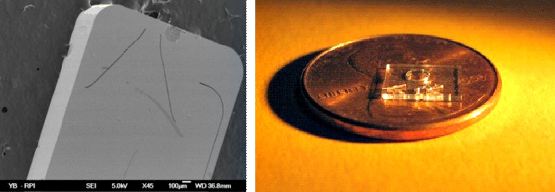
 In collaboration with one of our principal advisors, Professor Yves Bellouard (Eindhoven University of Technology), we have used these processes to machine micro-force sensors out of millimeter-thick fused silica wafers. The design consists of a flexure, made of two 40 micron-thin bars, that hold a central portion on which a V-groove is machined. The flexure has a low bending stiffness along the applied force direction (Z-direction). The flexure is used in its linear regime (small deflection).
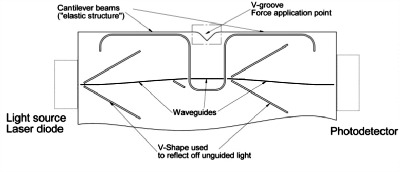
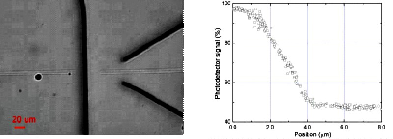
A subsurface optical waveguide divided in three portions is written below the surface and goes all the way across the structure along the X-axis (Figure 2 shows a close-view of the central portion of the waveguide). Once a force is applied on the V-groove, the flexure deflects along the Z direction and doing so, moves the central portion of the waveguide down. This misalignment between waveguides creates optical coupling losses at the interfaces. Through measurement of the optical loss one can extract the flexure position.
Further as the stiffness of the flexure is known one can calculate the force applied to the flexure.